What is a PCB?
A Printed Circuit Board, commonly known as a PCB, serves as the backbone of nearly all electronic devices. It provides both the physical structure and the electrical connections for electronic components, such as resistors, capacitors, and microcontrollers. By replacing bulky wiring with thin copper traces, PCBs make assemblies more compact, reliable, and easier to produce—in short, essential for modern electronics.
The Role of PCB Design
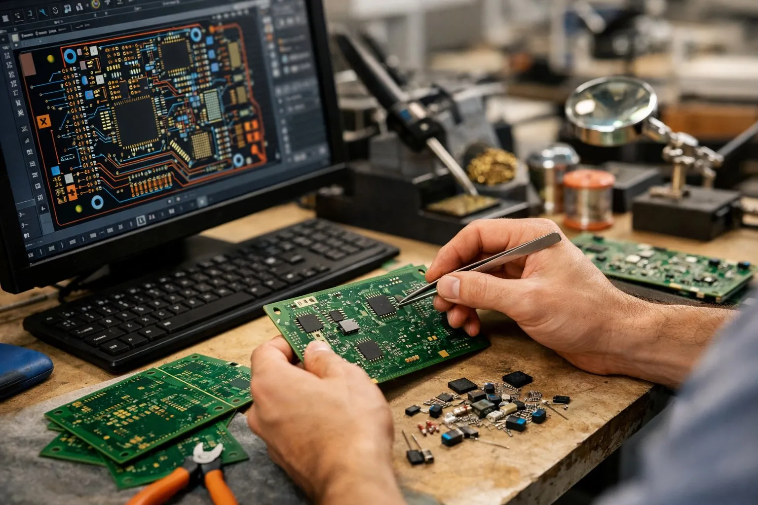
Before a PCB can be manufactured, it must be carefully designed. PCB design is a specialized form of electronic design automation (EDA) that involves creating a detailed digital layout of the board. Designers use software tools to place components, route traces, and define holes or cutouts. The resulting design ensures that all parts fit together functionally and physically, taking into account factors such as signal integrity, heat dissipation, and power distribution.
Key Steps in PCB Design
The design process typically starts with schematic capture: representing the electronic circuit in a symbolic diagram. Next, engineers create the board layout, where components are placed on a virtual board and interconnected via copper traces. Design rules—such as minimum trace width, spacing, and pad size—must be rigorously followed to avoid electrical faults or manufacturing problems.
Modern PCB design tools allow for error checking and simulation, helping to identify potential issues before production. Once the design is finalized, the software generates Gerber files, which are the industry-standard format for PCB fabrication instructions.
PCB Manufacturing Basics
After the design stage, the actual manufacturing of the PCB begins. This involves several steps: laminating thin copper sheets onto a non-conductive substrate, applying a photosensitive layer, and then using light to transfer the circuit pattern onto the board. Unexposed copper is etched away, leaving only the desired traces and pads. Additional processes include drilling holes for through-hole components, applying solder mask to protect the traces, and adding silkscreen markings for component placement.
Assembly and Testing
Once the bare PCB is manufactured, the next step is populating it with electronic components. This can be done manually for low-volume prototypes or with automated pick-and-place machines for large production runs. After assembly, the board undergoes testing to verify that all connections and functionalities work as intended. Functional and in-circuit tests help catch assembly errors or defective components before the final product reaches the customer.
Common Challenges in PCB Projects
PCB design and manufacturing involve a close interplay between creativity and practical constraints. Designers often face challenges like managing electromagnetic interference, optimizing for manufacturability, and staying within budget. It is also important to select suitable materials and ensure the design meets industry standards and regulatory requirements.
Choosing the right partner for your PCB needs, whether you are working with a local supplier or a global manufacturer, can make a significant difference in project success. For businesses looking for expertise in this area, collaborating with specialists in PCB design and manufacturing—such as those found at PCB—can streamline the process and help avoid costly mistakes.
Conclusion: The Foundation of Modern Electronics
Understanding the basics of PCB design and manufacturing is crucial for anyone entering the world of electronics, from hobbyists to engineers. With careful planning, the right tools, and reliable partners, you can create high-quality PCBs that serve as the foundation for innovative devices. Whether you are prototyping a new idea or scaling up to production, mastering these fundamentals will help you bring your electronics projects to life.
Written by
Tobias HargreaveNews editor and consumer tech writer, 14 years
Tobias spent 9 years on the news desk of a regional daily before moving into digital publishing, where he has edited more than 3,000 breaking news and explainer pieces. He now writes practical tips on staying informed, spotting weak sources and using news apps and alerts without the noise. He holds a journalism degree and runs a weekly fact check routine that he shares with readers.